The GPU Memory Hierarchy: L2, L1, and Registers
September 19, 2025
While High Bandwidth Memory (HBM) provides GPUs with massive throughput, it is still relatively far away from the compute units in terms of latency. To bridge that gap, modern GPUs employ a layered memory hierarchy: L2 cache, L1 cache (shared memory), and registers. Each layer trades capacity for speed, ensuring that the most frequently used data stays as close to the compute units as possible.
Why this Memory Hierarchy Matters
Training and inference involve repeatedly accessing weights, activations, and intermediate results. Fetching all of this directly from HBM would overwhelm its bandwidth and introduce unacceptable delays. By staging data through progressively faster and smaller memories, GPUs reduce both latency and energy consumption, keeping tensor cores and CUDA cores consistently fed.
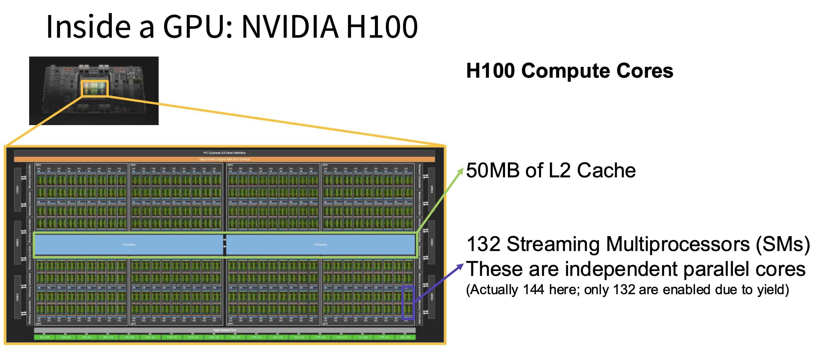
Figure 1: The inside of the compute core of the NVIDIA H100 GPU. We see 50MB of L2 cache as well as 132 streaming multiprocessors stacked next to each other.
L2 Cache - Global Buffer for All Streaming Multiprocessors (SMs)
The L2 cache sits on the GPU die but outside the SMs, as shown in Figure 1. It's shared across the entire GPU, meaning every SM can access it. In terms of size, we're talking about tens of megabytes — the NVIDIA A100 has 40 MB of L2, while the H100 bumps this up to 50 MB.
The L2 is much faster than HBM (tens of nanoseconds versus hundreds), though still slower than L1. Its main job is to hold recently accessed data from HBM so the GPU doesn't have to make repeated trips to the same location. If multiple SMs need the same model weights, the L2 acts as a shared buffer — only one trip to HBM is needed, and subsequent reads are served locally. This is especially helpful for large batch sizes or layers where the same weights are accessed by many different SMs.
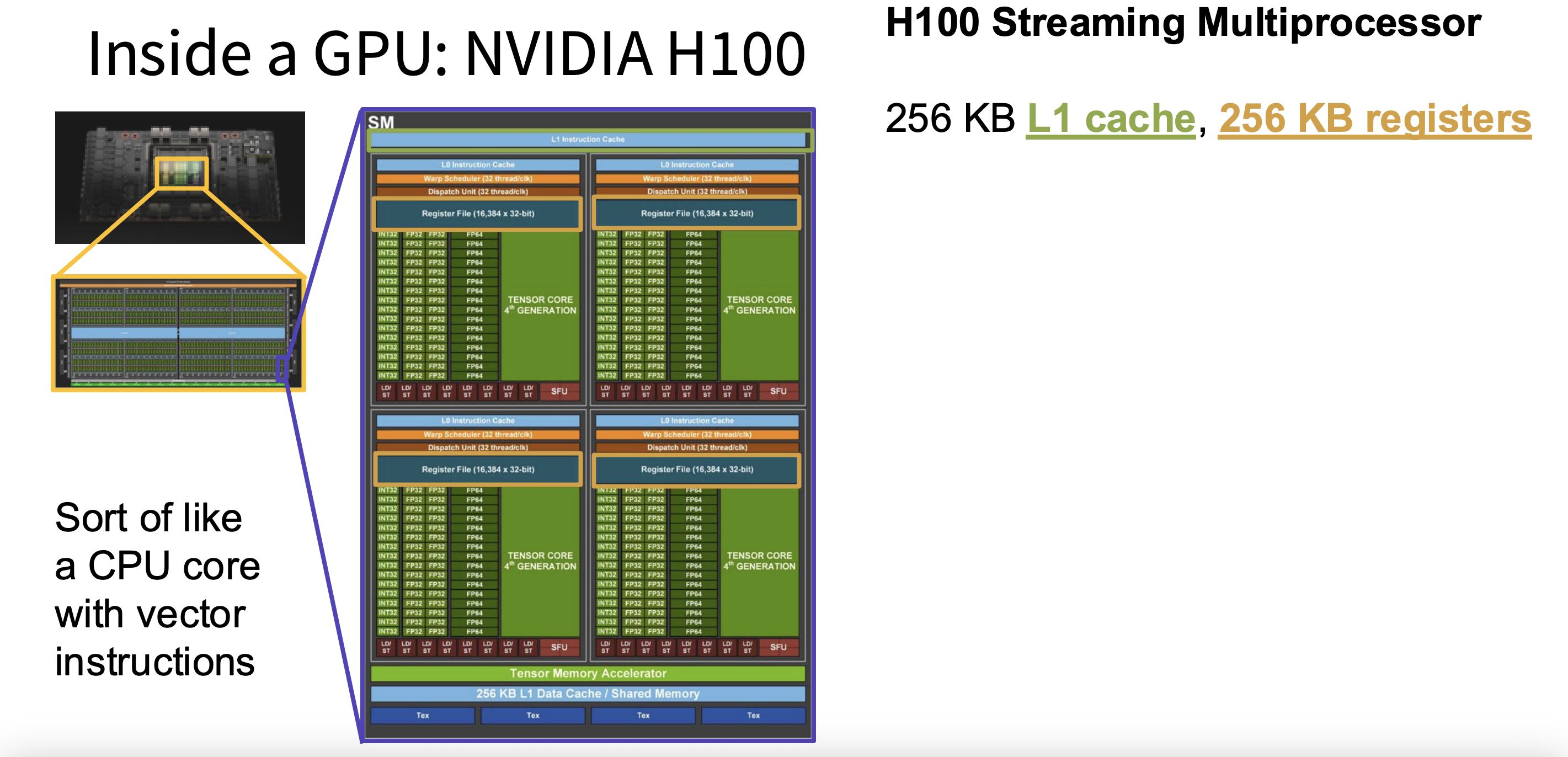
Figure 2: Inside the streaming multiprocessor (SM) of an H100, where we see the L1 instruction cache above.
L1 Cache (Shared Memory) — Local Fast Storage in Each SM
The L1 cache lives inside each SM and is private to that SM. It's small — around 128 KB per SM — but very fast, with access times of just a few nanoseconds. In CUDA, this memory can be split between an automatic cache and a programmer-managed region called shared memory, letting developers control exactly how data is reused.
This dual role makes L1 especially valuable. As a cache, it automatically holds recently loaded data so subsequent accesses don't have to reach all the way back to L2 or HBM. As shared memory, it lets all threads in a block collaborate — they load a shared piece of data once and reuse it many times. This is the foundation of tiled matrix multiplication: instead of each thread independently fetching its own inputs, the whole group cooperates to load a sub-tile into shared memory and reads from there. Without this, CNN kernels and matrix operations would flood the memory bus with redundant requests.
Registers — Per-Thread Working Memory
Registers are the fastest memory in the entire GPU — accessing them takes just a single clock cycle. They live directly inside each SM, tied to the CUDA and tensor cores, and each thread has its own private set that's invisible to other threads. While the total amount of register storage is large (the A100 has about 19 MB of registers in aggregate), each individual thread is limited to somewhere between 32 and 256 registers.
Every arithmetic instruction the GPU executes operates on values stored in registers. This includes the matrix elements being multiplied, loop counters, memory addresses, and intermediate sums that accumulate during computation. The key constraint is that if a thread needs more registers than are available, those values get "spilled" into L1 or L2, which is significantly slower. There's also a balancing act: the more registers each thread uses, the fewer threads can be active on the SM at once, which reduces parallelism. Efficient register usage is therefore a core part of writing high-performance GPU kernels.
How They Work Together in Large-Scale Training
Imagine training a transformer with billions of parameters. Here’s how the data actually moves through the hierarchy. First, model weights, activations, and optimizer states are pulled from HBM — the large but relatively slow memory pool on the GPU. From there, the fetched data lands in the L2 cache, where it’s accessible to all SMs. If multiple SMs end up needing the same weights (which is common), they can each read from L2 instead of hitting HBM again.
Next, within a specific SM, groups of threads (warps) copy sub-tiles of the matrix data into shared memory in L1. Multiple threads then reuse this shared copy to perform their portion of the matrix multiplication without any redundant memory fetches. Finally, each thread loads its specific operands into registers, and the tensor or CUDA cores consume those values to perform the actual multiply-accumulate operations. Intermediate results stay in registers until the computation is done, and then everything flows back up through the hierarchy: registers to L1, L1 to L2, and L2 back to HBM.